Global Semiconductor Bonding Market Report Size, Trends & Growth Opportunity, By Process Type, By Application, By Technology, By Type, By Region and forecast till 2027.
Report ID : QR1001451 | Industries : Semiconductors and Electronics | Published On :January 2022 | Page Count : 234Global Semiconductor Bonding Market
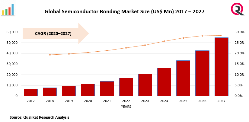
The global semiconductor bonding market was projected to grow from USD 887 million in 2020 to USD 1,059 million by 2027; it is expected to grow at a CAGR of 3.6% from 2020 to 2027.
Semiconductors’ arrangements comprise of atoms bonded together to form a homogeneous structure and it is used in the making of several integrated circuits (ICs) and fabrication devices. The structure of the material is homogeneous and virtually similar throughout in the bonding model.
Market Drivers
Key driving factor of the Semiconductor Bonding Market is the stacked die technology which is gaining acceptance in a range of electronics applications.
However, the growing demand for microelectromechanical systems (MEMS) is also another driving factor of the market.
Know more about this report: request for sample pages
Market Restraints
High operational cost of ownership is the key factor that restrain the growth of the Semiconductor Bonding Market.
Market Segmentation
Semiconductor Bonding Market is segmented into major 4 categories. Based on Process Type, the market is segmented into Die-To-Die Bonding, Die-To-Wafer Bonding and Wafer-To-Wafer Bonding. Based on Technology, the market is segmented into Die Bonding (Epoxy Die Bonding, Eutectic Die Bonding, Flip-chip Attachment, Hybrid Bonding) and Wafer Bonding (Direct Wafer Bonding, Anodic Wafer Bonding, TCB Wafer Bonding, Hybrid Bonding). Based on Type, the market is segmented into Die Bonder, Wafer Bonder and Flip-chip Bonder. Based on Application, the market is segmented into RF Devices, Mems and Sensors, Cmos Image Sensors, LED and 3D NAND. Based on Region, the market is segmented into North America, Europe, Asia Pacific, Latin America, Middle East.
Regional Analysis
Asia-Pacific is expected to be the dominant regional market because of the faster adoption of advanced technologies in developing countries in the region like China, Japan, India and as technical awareness in the Asia-Pacific is increasing, the market for consumer electronics also rising.
North America is also fast-growing region in the global semiconductor bonding market because of the huge demand for 3D semiconductor assembly and packaging solutions, the growing number of companies is adopting advanced technologies like IoT and artificial intelligence, mainly in the automotive sector.
Market Key Players
Some of the key players operating in Global Semiconductor Bonding Market are Shibaura Mechatronics, SUSS MicroTech SE, Yamaha Motor Robotics Corporation Co., Fuji Corporation, Panasonic, Kulicke & Soffa, ASM Pacific Technology Ltd., Shinkawa Ltd. and BE Semiconductor Industries NV.
Industry development
In October 2020, BE Semiconductor Industries N.V. (Besi) collaborated with Applied Materials, Inc. to develop the industry's first complete and proven equipment solution for die-based hybrid bonding, an emerging chip-to-chip interconnect technology that enables heterogeneous chip and subsystem designs for applications including high-performance computing, AI, and 5G.
In January 2021, ASM PACIFIC TECHNOLOGY (ASMPT) and EV GROUP (EVG) collaborated to create die-to-wafer hybrid bonding solutions for 3D-IC and heterogeneous integration applications. Chiplet technology combines chips with different process nodes into advanced packaging systems that can power new applications such as 5G, high-performance computing (HPC), and artificial intelligence. Die-to-wafer hybrid bonding is a key process for enabling the redesign of system-on-chip (SoC) devices to 3D stacked chips via chiplet technology—combining chips with different process nodes into advanced packaging systems that can power new applications such as 5G, HPC, and artificial intelligence (AI).
In April 2021, ASM PACIFIC TECHNOLOGY (ASMPT) introduced three new manufacturing systems that combine X-Celeprint's Micro-Transfer Printing (MTP) and ASM AMICRA's high precision die bonding technology to introduce the semiconductor industry's first complete system to enable high volume heterogeneous integration of ultra-thin dies onto up to 300mm base wafers.
Global Semiconductor Bonding Market TOC
1 Introduction
1.1 Objective of the Study
1.2 Market definition
1.3 Market Scope
2 Research Methodology
2.1 Data Mining
2.2 Validation
2.3 Primary Interviews
2.4 List of Data Sources
3 Executive Summary
4 Semiconductor Bonding Market Outlook
4.1 Overview
4.2 Market Dynamics
4.2.1 Drivers
4.2.2 Restraints
4.2.3 Opportunities
4.3 Porters Five Force Model
4.4 Value Chain Analysis
5 Network Security Market, By Process Type
5.1 Y-o-Y Growth Comparison, By Process Type
5.2 Semiconductor Bonding Market Share Analysis, By Process Type
5.3 Semiconductor Bonding Market Size and Forecast, By Process Type
5.3.1 Die-To-Die Bonding
5.3.2 Die-To-Wafer Bonding
5.3.3 Wafer-To-Wafer Bonding
6 Network Security Market, By Technology
6.1 Y-o-Y Growth Comparison, By Technology
6.2 Semiconductor Bonding Market Share Analysis, By Technology
6.3 Semiconductor Bonding Market Size and Forecast, By Technology
6.3.1 Die Bonding
6.3.1.1 Epoxy Die Bonding
6.3.1.2 Eutectic Die Bonding
6.3.1.3 Flip-chip Attachment
6.3.1.4 Hybrid Bonding
6.3.2 Wafer Bonding
6.3.2.1 Direct Wafer Bonding
6.3.2.2 Anodic Wafer Bonding
6.3.2.3 TCB Wafer Bonding
6.3.2.4 Hybrid Bonding
7 Network Security Market, By Type
7.1 Y-o-Y Growth Comparison, By Type
7.2 Semiconductor Bonding Market Share Analysis, By Type
7.3 Semiconductor Bonding Market Size and Forecast, By Type
7.3.1 Die Bonder
7.3.2 Wafer Bonder
7.3.3 Flip-chip Bonder
8 Network Security Market, By Application
8.1 Y-o-Y Growth Comparison, By Application
8.2 Semiconductor Bonding Market Share Analysis, By Application
8.3 Semiconductor Bonding Market Size and Forecast, By Application
8.3.1 RF Devices
8.3.2 Mems and Sensors
8.3.3 Cmos Image Sensors
8.3.4 LED
8.3.5 3D NAND
9 Network Security Market, By Region
9.1 Semiconductor Bonding Market Share Analysis, By Region
9.2 Semiconductor Bonding Market Share Analysis, By Region
9.3 Semiconductor Bonding Market Size and Forecast, By Region
10 North America Semiconductor Bonding Market Analysis and Forecast (2021-2027)
10.1 Introduction
10.2 North America Semiconductor Bonding Market Share Analysis, By Process Type
10.3 North America Semiconductor Bonding Market Size and Forecast, By Technology
10.4 North America Semiconductor Bonding Market Size and Forecast, By Type
10.4 North America Semiconductor Bonding Market Size and Forecast, By Application
10.5 North America Semiconductor Bonding Market Size and Forecast, By Country
10.5.1 U.S.
10.5.2 Canada
10.5.3 Mexico
11 Europe Semiconductor Bonding Market Analysis and Forecast (2021-2027)
11.1 Introduction
11.2 Europe Semiconductor Bonding Market Share Analysis, By Process Type
11.3 Europe Semiconductor Bonding Market Size and Forecast, By Technology
11.4 Europe Semiconductor Bonding Market Size and Forecast, By Type
11.4 Europe Semiconductor Bonding Market Size and Forecast, By Application
11.5 Europe Semiconductor Bonding Market Size and Forecast, By Country
11.5.1 Germany
11.5.2 France
11.5.3 UK
11.54. Rest of Europe
12 Asia Pacific Semiconductor Bonding Market Analysis and Forecast (2021-2027)
12.1 Introduction
12.2 Asia Pacific Semiconductor Bonding Market Share Analysis, By Process Type
12.3 Asia Pacific Semiconductor Bonding Market Size and Forecast, By Technology
12.4 Asia Pacific Semiconductor Bonding Market Size and Forecast, By Type
12.4 Asia Pacific Semiconductor Bonding Market Size and Forecast, By Application
12.5 Asia Pacific Semiconductor Bonding Market Size and Forecast, By Country
12.5.1 China
12.5.2 Japan
12.5.3 India
12.5.4. Rest of Asia Pacific
13 Latin America Semiconductor Bonding Market Analysis and Forecast (2021-2027)
13.1 Introduction
13.2 Latin America Semiconductor Bonding Market Share Analysis, By Process Type
13.3 Latin America Semiconductor Bonding Market Size and Forecast, By Technology
13.4 Latin America Semiconductor Bonding Market Size and Forecast, By Type
13.4 Latin America Semiconductor Bonding Market Size and Forecast, By Application
13.5 Latin America Semiconductor Bonding Market Size and Forecast, Country
13.5.1. Brazil
13.5.2. Rest of Latin America
14 Middle East Semiconductor Bonding Market Analysis and Forecast (2021-2027)
14.1 Introduction
14.2 Middle East Semiconductor Bonding Market Share Analysis, By Process Type
14.3 Middle East Semiconductor Bonding Market Size and Forecast, By Technology
14.4 Middle East Semiconductor Bonding Market Size and Forecast, By Type
14.4 Middle East Semiconductor Bonding Market Size and Forecast, By Application
14.5 Middle East Semiconductor Bonding Market Size and Forecast, By Country
14.5.1. Saudi Arabia
14.5.2. UAE
14.5.3. Egypt
14.5.4. Kuwait
14.5.5. South Africa
15 Competitive Analysis
15.1 Competition Dashboard
15.2 Market share Analysis of Top Vendors
15.3 Key Development Strategies
16 Company Profiles
16.1 Shibaura Mechatronics
16.1.1 Overview
16.1.2 Offerings
16.1.3 Key Financials
16.1.4 Business Segment & Geographic Overview
16.1.5 Key Market Developments
16.1.6 Key Strategies
16.2 SUSS MicroTech SE
16.2.1 Overview
16.2.2 Offerings
16.2.3 Key Financials
16.2.4 Business Segment & Geographic Overview
16.2.5 Key Market Developments
16.2.6 Key Strategies
16.3 Yamaha Motor Robotics Corporation Co.
16.3.1 Overview
16.3.2 Offerings
16.3.3 Key Financials
16.3.4 Business Segment & Geographic Overview
16.3.5 Key Market Developments
16.3.6 Key Strategies
16.4 Fuji Corporation
16.4.1 Overview
16.4.2 Offerings
16.4.3 Key Financials
16.4.4 Business Segment & Geographic Overview
16.4.5 Key Market Developments
16.4.6 Key Strategies
16.5 Panasonic
16.5.1 Overview
16.5.2 Offerings
16.5.3 Key Financials
16.5.4 Business Segment & Geographic Overview
16.5.5 Key Market Developments
16.5.6 Key Strategies
16.6 Panasonic
16.6.1 Overview
16.6.2 Offerings
16.6.3 Key Financials
16.6.4 Business Segment & Geographic Overview
16.6.5 Key Market Developments
16.6.6 Key Strategies
16.7 Kulicke & Soffa
16.7.1 Overview
16.7.2 Offerings
16.7.3 Key Financials
16.7.4 Business Segment & Geographic Overview
16.7.5 Key Market Developments
16.7.6 Key Strategies
16.8 ASM Pacific Technology Ltd.
16.8.1 Overview
16.8.2 Offerings
16.8.3 Key Financials
16.8.4 Business Segment & Geographic Overview
16.8.5 Key Market Developments
16.8.6 Key Strategies
16.9 BE Semiconductor Industries NV
16.9.1 Overview
16.9.2 Offerings
16.9.3 Key Financials
16.9.4 Business Segment & Geographic Overview
16.9.5 Key Market Developments
16.9.6 Key Strategies
16.10 Shinkawa Ltd.
16.10.1 Overview
16.10.2 Offerings
16.10.3 Key Financials
16.10.4 Business Segment & Geographic Overview
16.10.5 Key Market Developments
16.10.6 Key Strategie